

industry use cases - electronics & semiconductor manufacturingVision Systems in Electronics & Semiconductors
Let’s be honest. If you’re managing electronics or semiconductor production, you’re working in one of the most demanding environments in manufacturing. Every micron matters. A single misalignment, soldering error, or contamination can lead to catastrophic consequences—product failures, massive recalls, or worse, safety issues in critical applications.
With components shrinking, complexity increasing, and customer expectations climbing, the pressure to deliver flawlessly is real. And traditional inspection methods? They simply can’t keep up.
That’s where Datalogic’s vision systems make a real impact. Our advanced inspection solutions help you catch problems early, verify critical steps automatically, and scale your QA efforts across fast-moving production lines—without sacrificing precision or speed.
Let’s explore how vision systems are transforming electronics and semiconductor manufacturing:
The Challenge:
Modern PCBs are packed with hundreds, even thousands, of components—each requiring perfect placement. A single missing capacitor or misaligned microchip can turn a finished board into a scrap unit. And as boards get smaller, denser, and faster, manual spot checks just don’t cut it anymore.
How Vision Solves It:
✔ Detects the presence and correct positioning of all components, from tiny SMD resistors to complex BGA chips
✔ Confirms orientation, polarity, and placement tolerances in real-time
✔ Catches misfeeds, shadowed placements, or partially seated elements instantly
Implementation Example:
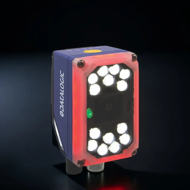
P-Series smart cameras scan PCBs immediately post-placement on the SMT line, cross-referencing placement data and highlighting errors before soldering begins.
The Challenge:
Invisible to the naked eye, solder issues like bridges, cold joints, or voids can silently kill an otherwise perfect circuit. With miniaturization, inspecting solder quality manually or with outdated AOI systems just isn’t reliable anymore.
How Vision Solves It:
✔ Measures solder shape, reflectivity, and uniformity with high-contrast imaging
✔ Identifies defects such as bridging, tombstoning, and insufficient fill
✔ Works seamlessly with pre- and post-reflow inspection workflows.
Implementation Example:
High-resolution modules inspect solder joints in QFN and BGA packages, ensuring reliable electrical connections before final testing and encapsulation.
The Challenge:
Every board, chip, and module must be traceable—but laser marking on reflective, curved, or miniature components is notoriously tricky. Poor contrast, misaligned characters, or missing codes mean lost traceability and compliance headaches.
How Vision Solves It:
✔ Reads and verifies laser-etched alphanumeric codes or data matrix identifiers
✔ Performs OCR/OCV even on difficult surfaces like matte black or shiny ICs
✔ Ensures each component is marked, readable, and correctly aligned.
Implementation Example:
Matrix 320 imagers scan ICs and PCBs post-marking to verify unique IDs and log them into the MES, enabling full product genealogy.
The Challenge:
Bent, missing, or misaligned pins are a silent killer in final assembly. They may pass unnoticed until the connector fails in the field—costing time, credibility, and warranty dollars.
How Vision Solves It:
✔ Counts and checks every pin or contact in real time
✔ Identifies pin deformation, offsets, or incorrect angles before assembly
✔ Works for surface mount and through-hole connectors across modules.
Implementation Example:
Vision cameras verify the integrity of USB-C, Ethernet, and board-to-board connectors before they’re enclosed—avoiding rework and improving field reliability.
The Challenge:
In the world of wafers and dies, defects can be microscopic—but their impact is enormous. Contaminants, scratches, and misaligned dies must be detected early to protect yield.
How Vision Solves It:
✔ Captures minute surface flaws, pattern distortions, or structural damage
✔ Enables inspection during wafer dicing, bonding, and packaging
✔ Integrates into cleanroom and particle-sensitive workflows.
Implementation Example:
High-resolution vision systems inspect die placement accuracy and wafer condition, reducing scrap during the back-end packaging process.
product storyDefect-Free PCB Inspection at 20,000 Units/Day
A global electronics brand manufacturing power management ICs and consumer modules was losing yield due to missed soldering defects and misaligned components. Their legacy AOI systems were slow, missed key defect types, and weren’t scalable across all lines.
⚠ Sampling inspection missed subtle solder faults and component polarity issues
⚠ Manual spot checks created bottlenecks during high-volume production shifts
⚠ Field returns were rising, impacting customer satisfaction and profitability
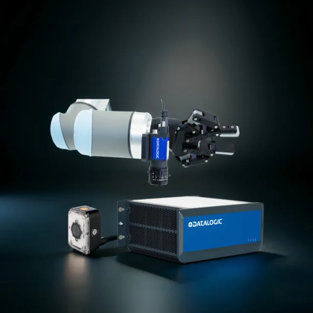
After implementing Datalogic’s P-Series smart cameras and MX-U processors across three SMT lines:
✔ They achieved real-time, full-board inspection at 20,000 units/day
✔ Inline alerts flagged component issues immediately, before reflow
✔ First-pass yield jumped 30% and field returns dropped by 60% within 90 days
With scalable vision inspection deployed across multiple lines, the company met its quality KPIs and cut rework costs dramatically—without slowing production.

featured resoursesDive Deeper into Vision for Electronics


FAQsEverything You Need to Know About Vision in Electronics
Can your systems handle reflective or metallic surfaces like solder or polished ICs?
Absolutely. Our systems include dome, coaxial, and structured lighting options to eliminate glare and capture clear images from shiny or uneven surfaces.
We use an MES—can we connect Datalogic vision systems to it?
Yes. Our platforms integrate seamlessly with MES, ERP, and PLC systems using standard industrial protocols like OPC UA, Modbus TCP, PROFINET, and EtherNet/IP.
How precise are your systems for microelectronics?
We offer smart cameras and sensors with resolutions up to 12MP and sub-pixel measurement capabilities—ideal for verifying fine-pitch components and micro-defects.
Do you support traceability and anti-counterfeiting requirements?
Definitely. Our systems verify serialized codes, capture inspection data, and create audit trails that support traceability, serialization compliance, and anti-counterfeit programs.
Can your solution grow with us as we scale new product lines?
Yes. Our modular hardware and software platform is designed for easy scaling. Whether you're adding new cameras, recipes, or inspection stages, your investment grows with you.
Vision Systems in Electronics & Semiconductor Manufacturing
Ready to Inspect Every Detail with Confidence?
Quality isn’t optional—it’s your reputation. Let Datalogic help you raise the bar with intelligent vision solutions that never miss a detail.