

industry use cases - retail & spparelPrecision Labelling for Precision Technology.
Ensure traceability, protect sensitive components, and accelerate production with labelling automation made for high-tech environments.
In electronics and semiconductor manufacturing, there’s zero margin for labelling errors. Whether you’re tracking components through assembly or sealing finished goods with tamper-proof codes, every label must be exact — in content, placement, and durability.
As a production or quality engineer, you’re navigating tight tolerances, ESD-sensitive environments, and ever-evolving traceability requirements. Manual labelling just isn’t sustainable at scale. That’s where Scan, Print & Apply comes in.
SPA gives you real-time, inline labelling precision — without slowing down your production flow or risking compliance slips.
Here’s how SPA is powering efficiency and traceability across electronics and semiconductor manufacturing:
The Challenge:
Every component — from chips to connectors — needs to be traced across your manufacturing lifecycle. But printing and applying traceability labels manually is slow, inconsistent, and prone to data errors. Add tight timelines and high mix, and it’s easy for mislabels to snowball into major quality issues.
How SPA Solves It:
✔ Prints and applies traceable barcodes/QR codes inline and in real time
✔ Connects directly to your MES/ERP for serial, lot, and part number integration
✔ Maintains accuracy across high-mix, high-speed production lines
Implementation Example:
A PCB manufacturer uses SPA to apply 2D DataMatrix labels on assembled boards. Each label is serialized and linked to a complete digital record before the board moves to final test
The Challenge:
Many components and assemblies are sensitive to electrostatic discharge. Even minor label handling can introduce risk — and basic labelling systems often overlook ESD safety protocols.
How SPA Solves It:
✔ Uses ESD-safe label stock and applicator components
✔ Operates with minimal human contact in ESD-controlled zones
✔ Applies anti-static warning labels and compliance IDs where needed
Implementation Example:
A microchip packaging line uses SPA to apply warning and compliance labels inside an EPA (electrostatic protected area), keeping components protected and compliant.
The Challenge:
You’re handling a mix of product formats — boards, reels, trays — all requiring precise labelling at different stages. Manual changeovers are inefficient and create room for misapplication.
How SPA Solves It:
✔ Applies small-format labels precisely on uneven, delicate, or contoured surfaces
✔ Switches formats and label types automatically based on product ID
✔ Reduces handling and eliminates relabelling due to misplacement.
Implementation Example:
An SMT line uses SPA to label reels with batch IDs and feeder locations. Labels are applied as reels enter the feeder stage, preventing delays downstream.
The Challenge:
Label data often changes mid-run, depending on what component is coming down the line. Manual relabelling just can’t keep up with that kind of variability.
How SPA Solves It:
✔ Instantly adjusts label content based on a scanned board, tray, or module ID
✔ Applies ID, revision, or process-specific info in real time
✔ Eliminates label mismatches due to manual entry or guesswork.
Implementation Example:
A module assembly station uses SPA to apply configuration-specific labels based on a pre-scan. Each label reflects the component’s exact specs and destination.
The Challenge:
Once an item leaves your facility, you need assurance it won’t be opened or tampered with. Manual placement of security labels is often inconsistent and lacks verification.
How SPA Solves It:
✔ Applies tamper-evident labels with accurate positioning
✔ Supports serialized or encrypted codes for post-sale verification
✔ Verifies label presence and adhesion inline.
Implementation Example:
A smartphone manufacturer uses SPA to seal each device’s packaging with a serialized, tamper-evident label. Labels are logged into the customer support system for future verification.
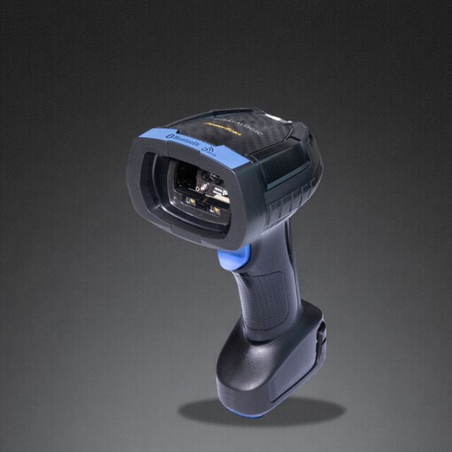
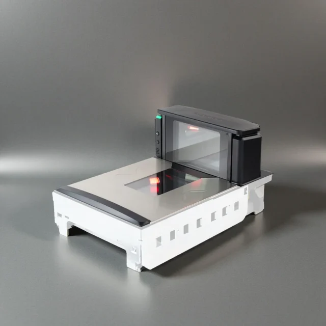
productsSPA Solutions Tailored for Electronics & Semiconductors

product storyHow SPA Eliminated Relabelling and Boosted Traceability for a PCB Manufacturer
Here’s the scenario: A major PCB supplier was losing time and traceability on the shop floor. Mislabelled boards had to be relabelled mid-process, delaying testing and creating audit gaps.
⚠ Operators were printing static labels in batches, causing SKU mismatches
⚠ Some labels didn’t hold through washing or reflow processes
⚠ Production had to pause for manual relabelling and data entry
After integrating SPA:
✔ 100% inline traceability — every board labelled and logged in sequence
✔ Durable labels withstand all cleaning and assembly phases
✔ 25% reduction in floor rework, with zero manual relabelling required
SPA gave them back control — speeding up production while tightening compliance.

featured resoursesDive Deeper into SPA for Electronics & Semiconductors


FAQsEverything You Need to Know About SPA in Electronics
Can SPA work with ESD-sensitive components?
Yes — we offer ESD-compliant applicators and label materials safe for use in EPAs and cleanrooms.
What kind of label sizes can it handle?
From micro 5mm labels to full reel or board labels — SPA systems are built for high-resolution, compact formats.
Is it compatible with MES or WMS systems?
Absolutely. Our solutions integrate seamlessly via API, OPC-UA, or middleware with your MES, ERP, or WMS.
What about label durability?
We support label stocks that withstand wash cycles, heat, and solvent exposure — ideal for PCB and final assembly lines.
Can it help with anti-counterfeit protection?
Yes. SPA can print serialized, encrypted, or QR-authenticated labels for tamper-proof sealing and warranty tracking.
Scan, Print & Apply in Electronics & Semiconductors